
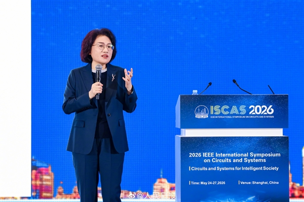
Huawei, (GNP): Huawei has introduced a new idea called the Tau Scaling Law to help improve the future of computer chips and semiconductor technology. The announcement was made during a technology conference in Shenzhen, where the company explained its plans for future chip development and advanced computing systems.
According to Huawei, the Tau Scaling Law is a new method that could help make computer chips much more powerful and efficient in the future. The company believes that chips developed using this new system could reach transistor density levels similar to 1.4-nanometer technology by 2031. In simple words, this means future Huawei chips could become smaller, faster, and more powerful.
This announcement is important because the semiconductor industry is facing major challenges. For many years, companies followed Moore’s Law, which stated that the number of transistors on a chip would continue to increase over time. However, as chips become extremely tiny, it is becoming harder and more expensive to keep improving them using traditional methods.
Huawei says the Tau Scaling Law offers a new direction for the future of chip technology. The company explained that the new approach is not only about fitting more transistors onto chips, but also about improving system architecture, saving energy, and increasing computing performance. These improvements are especially important for technologies like artificial intelligence, cloud computing, telecommunications, smart devices, and industrial automation.
Huawei also highlighted the importance of semiconductor innovation for the global digital economy. The company said advanced chips are necessary for future technologies such as self-driving systems, AI tools, next-generation communication networks, and smart industries.Technology experts see this announcement as a sign that Huawei wants to remain a major player in the semiconductor and AI industries despite international restrictions and growing geopolitical tensions. Due to limits on access to foreign chip technologies, Huawei has increased its investment in local research and independent innovation.
Also Read: Asia-Pacific Hit Hard by Ransomware in 2025
Company officials stated that the Tau Scaling Law is the result of many years of scientific research and engineering work. Huawei also emphasized the importance of cooperation between engineers, universities, researchers, and industry partners to speed up future chip development.If Huawei successfully achieves transistor densities similar to 1.4-nanometer technology, it would represent a major advancement in semiconductor manufacturing. Smaller transistors usually allow chips to work faster, use less electricity, and handle more advanced computing tasks.
Huawei’s announcement also shows that the larger global competition in semiconductor technology. Many countries and technology companies are currently investing heavily in artificial intelligence, advanced chip manufacturing, and powerful processors because these technologies are considered essential for future economic growth and digital transformation.
During the conference, many technology experts and industry leaders described the Tau Scaling Law as a bold and motivated step toward the future development of semiconductor scaling and computing technology.
Huawei ended the presentation by repeating its commitment to research and innovation. The company stated that continuous investment in advanced chip technologies will play an important role in shaping the future of global connectivity, AI, and digital infrastructure.