Samsung (GNP): Samsung Electronics has announced a major innovation in semiconductor technology with the development of its innovative 3D Stacked Field-Effect Transistor (FET) architecture, a significant advancement that could redefine the future of next-generation chip manufacturing.
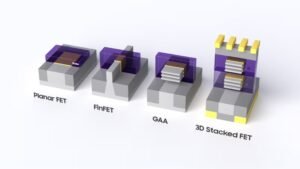
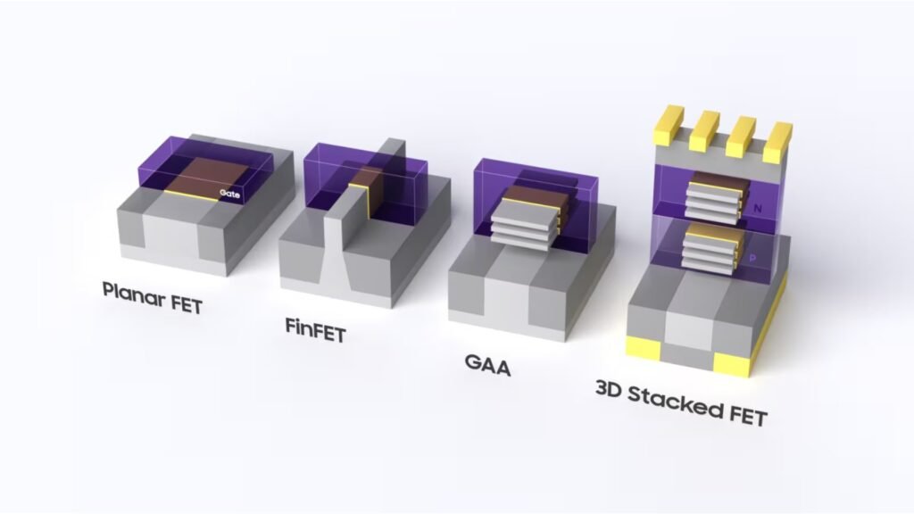
The South Korean technology leader revealed that its new approach moves beyond conventional two-dimensional chip designs by vertically stacking transistor structures. This innovation allows semiconductor engineers to increase transistor density, improve performance, and enhance power efficiency while reducing the physical footprint of advanced chips.
More, semiconductor manufacturers place n-type and p-type transistors side by side on a flat, two-dimensional surface. Also this design has enabled decades of technological progress, it is increasingly approaching its physical limitations as the demand for faster, smaller, and more efficient chips continues to grow.
Samsung’s new 3D Stacked FET technology addresses these challenges by placing transistor components vertically, creating a three-dimensional architecture that maximizes available space.
According to Samsung, one of the most important advantages of the new technology is its ability to dramatically increase transistor density. By stacking transistor structures rather than arranging them side by side, engineers can fit more components into the same chip area, enabling the development of more powerful processors without increasing chip size.
The breakthrough also promises substantial improvements in power efficiency and overall performance. Samsung’s design incorporates triple-stacked nanosheet channels, allowing electrical signals to move more effectively through the transistor structure. This approach helps optimize energy consumption while delivering higher computational capabilities, making the technology particularly valuable for future applications in artificial intelligence, high performance computing, mobile devices, and data centers.
Also Read: Apple Price Hikes 2026 Coming From Rising Memory Costs
Industry experts view three-dimensional transistor architectures as one of the most promising paths for extending semiconductor scaling beyond the limits of traditional manufacturing methods. As demand for advanced computing continues to accelerate worldwide, innovations such as Samsung’s 3D Stacked FET technology could play a crucial role in enabling future generations of electronic devices and digital infrastructure.
This achievement has already received international recognition. Samsung’s research paper detailing the technology was awarded the prestigious Best Paper Award at the 2026 VLSI Symposium, one of the semiconductor industry’s leading scientific conferences. The paper reportedly earned an impressive rating of 8.29 out of 10, reflecting strong recognition from experts and researchers in the field.
The award highlights Samsung’s continued investment in semiconductor research and development and reinforces its position as a global leader in advanced chip technologies. The company has consistently pursued innovations aimed at overcoming technological barriers and supporting the rapidly evolving needs of the digital economy.
As industries increasingly rely on powerful computing solutions, efficient artificial intelligence systems, and energy-conscious technologies, breakthroughs in chip architecture are becoming more important than ever. Samsung’s latest innovation demonstrates how advanced engineering can help meet these growing demands while opening new possibilities for the future of semiconductor manufacturing.
With the successful development of 3D Stacked FET technology, Samsung has taken a important step toward shaping the next era of computing, providing a foundation for faster, smarter, and more efficient electronic devices in the years ahead.